To scan objects and analyze light across the electromagnetic spectrum, not just the visible bands, we use Hyperspectral Imaging (HSI). Through HSI, users can obtain high-definition images and identify otherwise invisible objects and materials in industries such as agriculture, manufacturing, biology, biomedical imaging and geosciences.
例如,drone-mounted HSI相机可以扫描acres of crops to identify signs of disease, water stress or reduced soil quality that would otherwise go undetected by the naked eye. This enables farmers to take action and maintain yields while utilizing resources, like water and fertilizer, more efficiently. The ability to create real-time, snapshot-like video images with a moving camera is essential for scanning large areas, like the fields farmers grow their crops in. Traditional linescan, also known as push-broom, hyperspectral cameras are slower and more complicated, and therefore too expensive for applications such as crop monitoring.
Imec Develops Hyperspectral Imaging Camera Using SPTS Deep Oxide Etch Technology
Imec, a world-leading R&D and innovation hub in nanoelectronics and digital technologies, developed on-chip technology which makes hyperspectral imaging real-time, compact and scalable. Spectral filters, tailored to the needs of the user, can be manufactured directly onto image sensor pixels at the wafer level.
“Last year in imec, we were struggling to enable new projects using complex filter stacks. So we initiated a demo with SPTS on their Synapse module for thick filter stack etches. The SPTS Process Team found a working process and provided excellent results summary, and we are now ready to start filter stack etch in the newly installed Synapse chamber in imec.”
– Reda Boufadil, imec Area Manager for Dry Etch
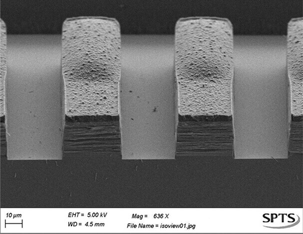
These spectral filters include thick stacks of alternating materials with high and low refractive index on a silicon or quartz wafer. Trench features between 3µm and 20µm deep were required, etched through the filter stack. Due to the low volatility of the layers, SPTS recommended their Synapse™ etch technology for this application, with its high ion density to ensure a productive etch rate and directionality.

22µm deep trenches through SiO2-metal oxide filter stack on Si wafer
As well as etch depth and sidewall profile, other factors such as good cross-wafer uniformity and end-point control were important to ensure Imec could develop a production-worthy manufacturing route with high yields. Read more aboutSPTS plasma etch technologyand its other applications inphotonics, as well as its use inadvanced packaging,RFandpower device manufacturing.
Follow Us On
Tags:SPTS