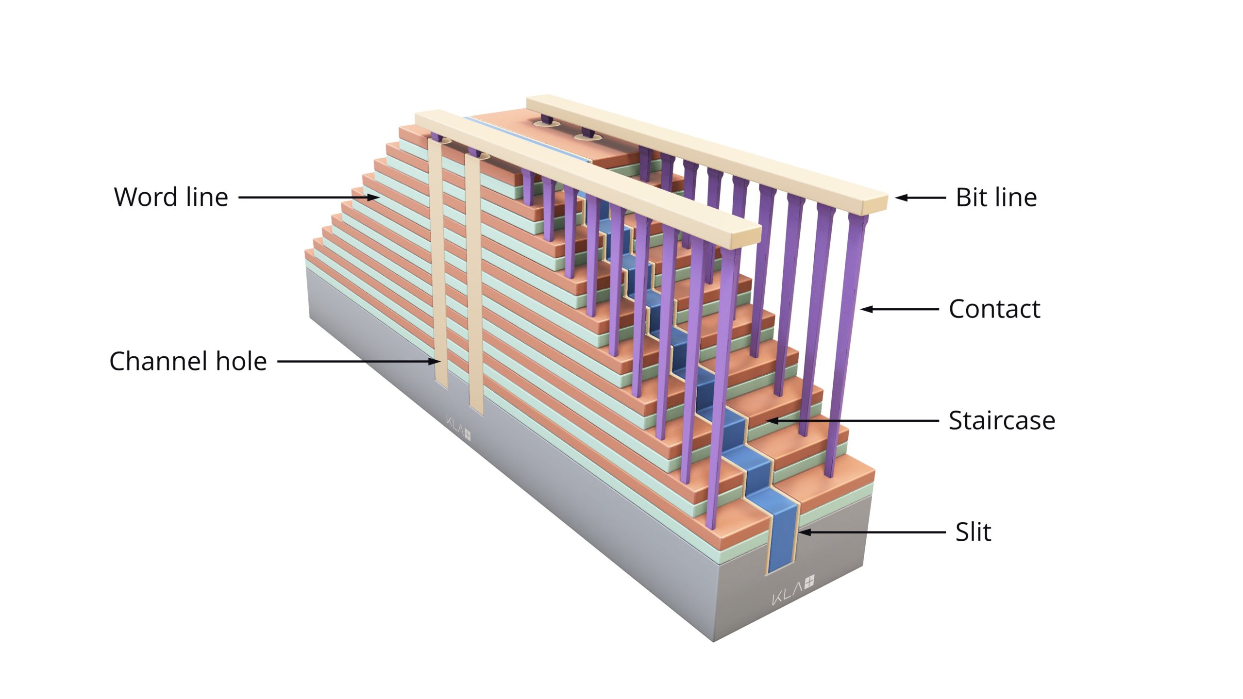
3D NAND memory is pervasive in today’s electronics – mobile devices, laptops, data centers, automobiles, and USB drives are just some of the places where 3D NAND provides fast, efficient data storage. This non-volatile, low-cost memory is comprised of a structure much like a miniature skyscraper, built at the nanoscale level with extraordinary precision. The primary structure of 3D NAND is created by first alternating film depositions – creating a film stack that can be >96 layers thick. Then, memory channel holes are created with a high aspect ratio (HAR) etch, exceeding 100:1, through the entire film stack. To achieve space efficiency and cost effectiveness, each new node in 3D NAND takes the skyscraper even higher, with more film layers creating an ever higher vertical stack.

One of the challenges for 3D NAND manufacturing is that the construction of these extreme film stacks can distort the wafer causing wafer shape non-uniformity, wafer stress and wafer warp: instead of being flat like a pancake, the wafer becomes distorted like a potato chip. As the height of the film stack has increased, the extent of potential wafer bowing has also increased. In order to understand and control this warp, 3D NAND manufacturers have implemented process monitoring strategies that track the bow and warp of wafers to ensure they meet specifications for downstream process steps. Announced today, KLA’snew PWG5™ patterned wafer geometry systemis the industry-standard for inline monitoring of wafer shape, stress and warp during 3D NAND, advanced DRAM and leading-edge logic IC manufacturing.

Our team of engineers and scientists developed multiple technologies – from optical subsystems to an advanced compute architecture and algorithms – to ensure the PWG5 provides IC manufacturers with metrology capability that contributes to their success. These technological innovations come together to produce comprehensive wafer geometry data that helps fab engineers understand their processes and move their IC innovations from concept to production.
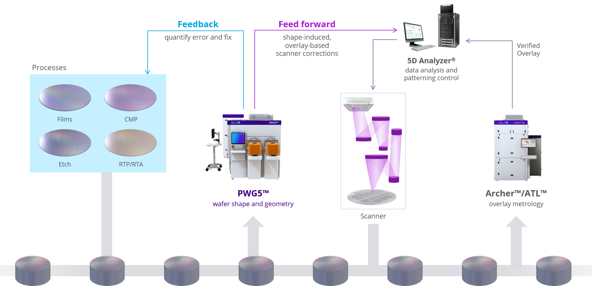
Addressing one critical need of IC manufacturers, the PWG5 provides the industry’s best dynamic range for wafer warp measurement, supporting inline monitoring and control of wafer warp levels that can be as high as 1000µm. This allows IC manufacturers to quickly identify process-induced wafer distortion that can have an adverse effect on patterning. PWG5 wafer shape data is used by fab engineers to drive decisions that improve device processing: re-work the wafer, implement process tool corrections or feed data forward to subsequent processes.
For example, there is a direct correlation between intra-die stress and overlay error: small deviations in the alignment of layer-to-layer device patterns can affect device performance. Monitoring intra-die stress requires measuring with high data density and high resolution, which the PWG5 system provides via the combination of high numerical aperture (NA) optics and small pixel size. Operating in a high volume manufacturing (HVM) environment, the system can quickly collect wafer geometry data, enabling process and patterning corrections that improve device performance.

Integrating PWG5 with KLA’s 5D Analyzer®gives process engineers the ability to improve on product overlay by correlating wafer shape to overlay residuals and identifying process induced wafer shape variations. By importing PWG5 data to 5D Analyzer, engineers can understand what adjustments need to be made to scanners to compensate for shape induced overlay errors. This integration also enables real-time feed forward of wafer shape data to the scanner to address overlay errors due to wafer stress. This is particularly helpful for 3D NAND where thick film stacks can distort wafers.
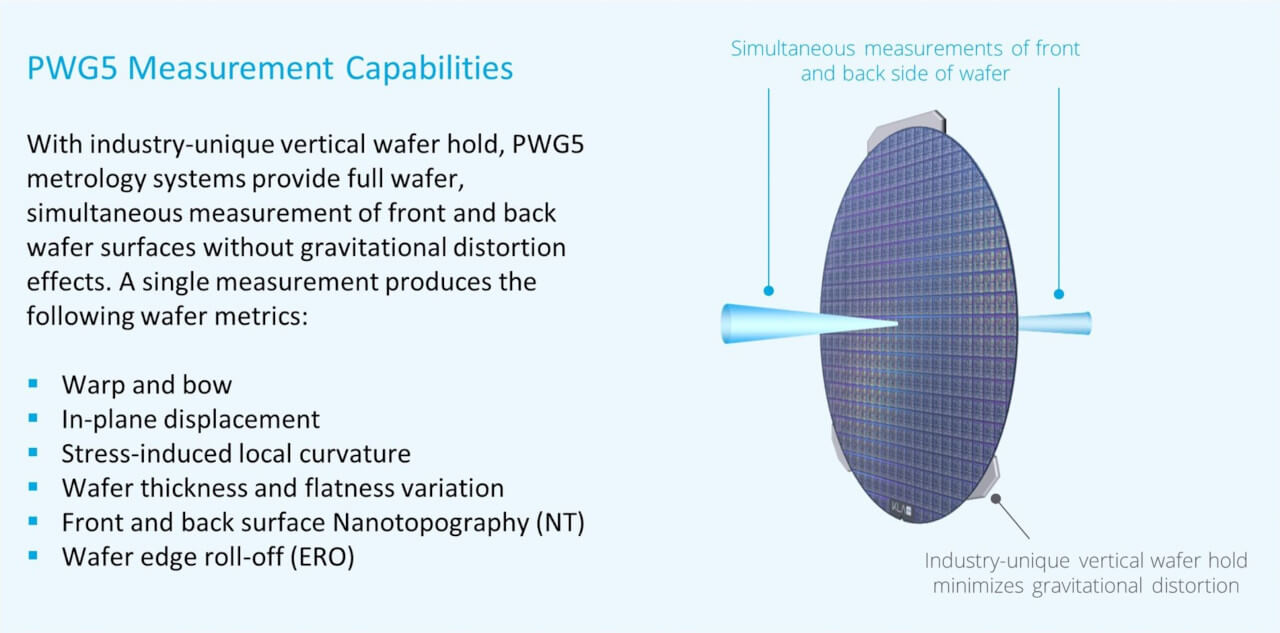
The PWG5 supports high volume production by providing multiple metrics in a single measurement for both bare and unpatterned wafers, including shape, thickness, front and back nano-topography and edge roll off (ERO). In addition, the industry-unique and gravity distortion-free vertical wafer hold system produces state-of-the-art precision, matching, measurement accuracy and reliability for a range of process control and monitoring applications.

KLA’s PWG5 system, built on the industry-standard WaferSight™ platform, is the complete wafer geometry control solution for both patterned and unpatterned wafers for ≥96 layer 3D NAND devices and ≤1Xnm logic and DRAM design nodes.
有关PWG5图案晶圆几何系统的更多信息,请访问产品页面, see ourpress release,或访问我们的虚拟展位Semicon Japan!
Follow Us On